PCB stack-up
Multilayers
Rigid PCB stack up
Our standard multi-layer PCB stackup is predominantly made up of
three components
with varying thicknesses of Copper Foil, Pre-preg and Copper
clad FR4 laminates as cores
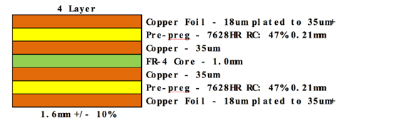
Multilayers
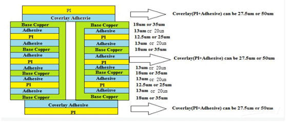
FPC stack-up
Multilayers Flexible circuit boards stack-up , PI ,base copper with or
without adhesive
,overlay , the thickness is from 0.15mm-0.5mm.
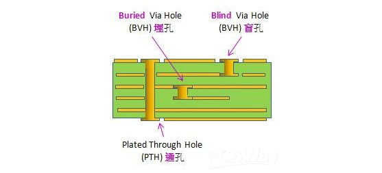
Blind Vias
: connects an
inner layer with the adjacent surface layer, they are only
visible on one side
of the boards and so are called ‘blind’ Vias.
Buried
Vias: Connects two adjacent inner copper
layers. They are not visible from
the surface and so are ‘buried’
Copper
in the wall of PTH
The thickness of copper in the wall of PTH hole as 25 at least
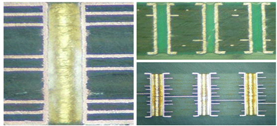
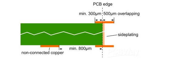
Side
Plating
To guarantee the producibility of the side plating, the metallized
area must be
defined using overlapping copper (copper surface, pads, or tracks) in the CAD
layout. Minimum
overlap:500um On the connected layer, min 300um of connected
copper must be
defined. On non-connected layers, the copper should have gap of
min. 800um
from the outer contour